搜索
Close this search box.

GaSb Wafer

Additional information

Wafer Size

2inch to 4inch(50 to 100mm)

Growth Method

VGF method

Orientation

100,111

Wafer Thickness

500-800um or per request

TTV (μm)

<20um or per discuss

Type/Dopant

Te dope or Zn dope

Carrier density

(1-100)E17

Mobility

200-3500

Product Introduction

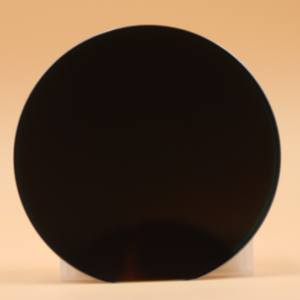
GaSb wafer is a III-V chemical compound semiconductor wafer, which is very critical material in infrared detector and infrared sensor application of its high sensitivity, long life, long lightweight, and great reliability. the spectral range for GaSb material can reach 4um area.

Send A Request or Inquiry

We will contact you as soon as possible, please pay attention to the email with the suffix “@rewinmc.com”